The 20 pin gate array used in the 1541B and 1571 disk drives is
designed to work in conjunction with the 40/42 pin gate array
also used in these drives. As illustrated in the block diagram,
this I.C. controls 3 operations:
1. ADDRESS SELECTOR
The function of the address selector is to produce ROM, RAM and
I/O chip select signals by decoding the addresses A10, A12, A13,
A14 and A15. The system clocks are not gated with the address
lines in this I.C. All chip select outputs are ACTIVE LOW.
Address Decode Map:  RAME   0000 -- 07FF
                     IO1    1800 -- 1BFF
                     IO2    1C00 -- 1FFF
                     CS1    2000 -- 3FFF
                     CS2    4000 -- 7FFF
                     ROME   C000 -- FFFF
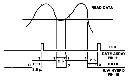
This correction signal is generated during the period that the
data pattern is two consecutive zeros. With the Commodore GCR
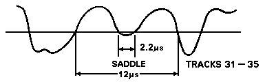
type recording format, a problem occurs in the waveform of the
read signal. In the worst case pattern of 1001, a saddle
condition will occur as illustrated below.
The worst case saddle will occur in tracks 31 to 35 and if not
compensated for, will result in a read error. In the original
1541 drives, a one-shot was used to correct the condition;
however, in this gate array it is corrected digitally.
The data output line, pin 19, of the R/W Hybrid's data comparitor
is fed to the data input line, pin 3, of this gate array.
The data is then compared with the last data value which has been latched by the gate array, 2.6 usec after the rising or falling edge of the data line. If the current data value differs from the previous data value, the clear line is set to a high level for a duration of 63 nsec. If the values are the same, the clear line is not set.